Axion® T2000: X-Ray Vision for Vertical Memory Devices
Dec 6, 2022
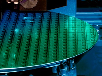
KLA’s new Axion® T2000 metrology system harnesses the power of X-rays to measure the complex vertical structures that form advanced memory chips....

Our process-control and process-enabling solutions are designed to boost the innovation speed of the electronics industry. We help our customers achieve leading-edge performance.
Dec 6, 2022
KLA’s new Axion® T2000 metrology system harnesses the power of X-rays to measure the complex vertical structures that form advanced memory chips....
Apr 12, 2022
Extreme ultraviolet (EUV) lithography is a key technology inflection for the semiconductor industry. While shifting the scanner wavelength to EUV...
Apr 7, 2022
Imagine if manufacturers could reduce design-for-manufacturability (DFM) analysis time by 96% and, ultimately, the time to market for complex PCBs....
Jan 25, 2022
The KLA Instruments™ portfolio of optical profiler tools are widely used in the industry due to their rapid measurement time...
Sep 21, 2021
Chip manufacturing is a journey of a thousand process steps. Each step requires extreme precision and control in order to...
Jun 22, 2021
KLA is committed to helping the automotive industry achieve strict electronics quality standards. To this end, we’ve unveiled four new...
You've selected to view this site translated by Google Translate.
KLA China has the same content with improved translations.
Would you like to visit KLA China instead?
您已选择查看由Google翻译翻译的此网站。
KLA中国的内容与英文网站相同并改进了翻译。
你想访问KLA中国吗?
If you are a current KLA Employee, please apply through the KLA Intranet on My Access.